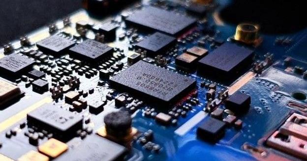
When it comes to designing electronic projects, one of the critical decisions you’ll need to make is choosing the type of printed circuit board (PCB) to use. PCBs come in various configurations, but one of the most common choices is the 2-layer PCB. In this article, we will explore the advantages and disadvantages of using 2 layer PCBs for electronic projects and provide tips on how to design them effectively.
Understanding 2 Layer PCBs
A 2 layer PCB, as the name suggests, consists of two layers of conductive material separated by an insulating layer (substrate). These PCBs are widely used in various electronic applications due to their simplicity and cost-effectiveness. Each layer of the PCB can contain traces, components, and other electrical elements that make the circuit work.
Advantages of 2 Layer PCBs
- Cost-Efficiency
One of the most significant advantages of 2 layer PCBs is their cost-effectiveness. They are less expensive to manufacture compared to multilayer PCBs, making them a budget-friendly choice for many electronic projects, especially those with simpler circuitry.
- Easy to Prototype
2 layer PCBs are ideal for prototyping because they are readily available and can be quickly produced. This is crucial for engineers and hobbyists who need to test their designs before moving on to more complex and expensive PCB types.
- Shorter Design Time
Designing a 2 layer PCB is generally less time-consuming than designing a multilayer PCB. This is because there are fewer layers to consider, which simplifies the design process and reduces the chances of errors.
- Simplicity and Reliability
2 layer PCBs are less prone to signal interference and noise compared to multilayer PCBs. With fewer layers, it is easier to troubleshoot and identify issues, leading to more reliable performance.
- Versatility
2 layer PCBs are versatile and can be used in a wide range of applications. Some common examples include:
- Consumer Electronics: Devices like smartphones, calculators, and remote controls often use 2 layer PCBs for their simplicity and cost-effectiveness.
- Industrial Control Systems: Many industrial control systems and automation equipment rely on 2 layer PCBs to control various processes.
- LED Lighting: LED drivers and control boards frequently use 2 layer PCBs due to their reliability and cost-efficiency.
Disadvantages of 2 Layer PCBs
- Limited Routing Space
One of the main drawbacks of 2 layer PCBs is their limited routing space. With only two layers available for traces and components, it can be challenging to design complex circuits with a high density of components.
- Reduced Signal Integrity
2 layer PCBs may struggle with signal integrity in high-frequency applications. The limited number of layers can lead to signal crosstalk and interference, affecting the performance of sensitive electronic devices.
- Ground Plane Limitations
In multilayer PCBs, additional layers can be dedicated to a ground plane, which helps in reducing electromagnetic interference (EMI) and providing a stable reference point for signals. In 2-layer PCBs, there is limited space for a dedicated ground plane, which can be a disadvantage in EMI-sensitive applications.
- Complex Designs May Require More Layers
For projects with complex circuitry or high-speed data transmission requirements, a 2 layer PCB may not be sufficient. In such cases, engineers may need to consider more advanced PCB options, which can be costlier and require specialized manufacturing processes.
Tips for Effective 2-Layer PCB Design
To maximize the advantages of 2 layer PCBs while minimizing their limitations, here are some tips for effective design:
- Plan Your Layout Carefully: Efficient component placement and trace routing are critical. Plan the layout to minimize signal crosstalk and interference.
- Use Ground Planes Wisely: While 2-layer PCBs have limited space for ground planes, try to allocate a portion of the PCB to ground connections to improve signal integrity.
- Keep Signal Paths Short: Shorter signal paths reduce the chances of signal degradation. Minimize the length of traces to maintain signal integrity, especially in high-frequency applications.
- Consider Stacked Vias: Stacked vias allow you to make connections between layers, which can be helpful for routing traces and connections in tight spaces.
- Use High-Quality Materials: Select high-quality PCB materials to improve the overall reliability of your design.
- Perform Thorough Testing: Before finalizing your design, conduct thorough testing and troubleshooting to identify and rectify any issues.
Conclusion
In the world of electronic design, choosing the right PCB type is crucial for the success of your project. 2 Layer PCBs offer several advantages, including cost-efficiency, ease of prototyping, and simplicity. However, they do come with limitations, such as limited routing space and reduced signal integrity in high-frequency applications.
When deciding whether to use a 2 layer PCB for your project, consider the complexity of your circuit, budget constraints, and the specific requirements of your application. By following effective design practices and taking advantage of the versatility of 2 layer PCBs, you can create reliable electronic projects that meet your needs.


